Use ARM Assembly to Implement i2c Communication
Project Overview
This document presents the final individual project for EEE 5264, Advanced Microprocessors, at Lawrence Technological University. The project, requiring the implementation of a real-world task using ARM assembly, culminated in a 15-minute technical demonstration to the class. The course focused on the design and application of ARM microcomputers, with a strong emphasis on ARM assembly language programming.
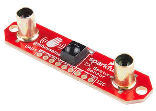
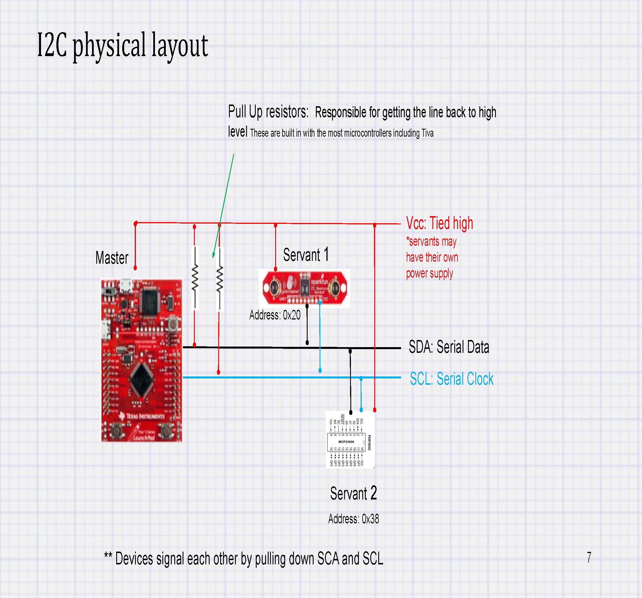
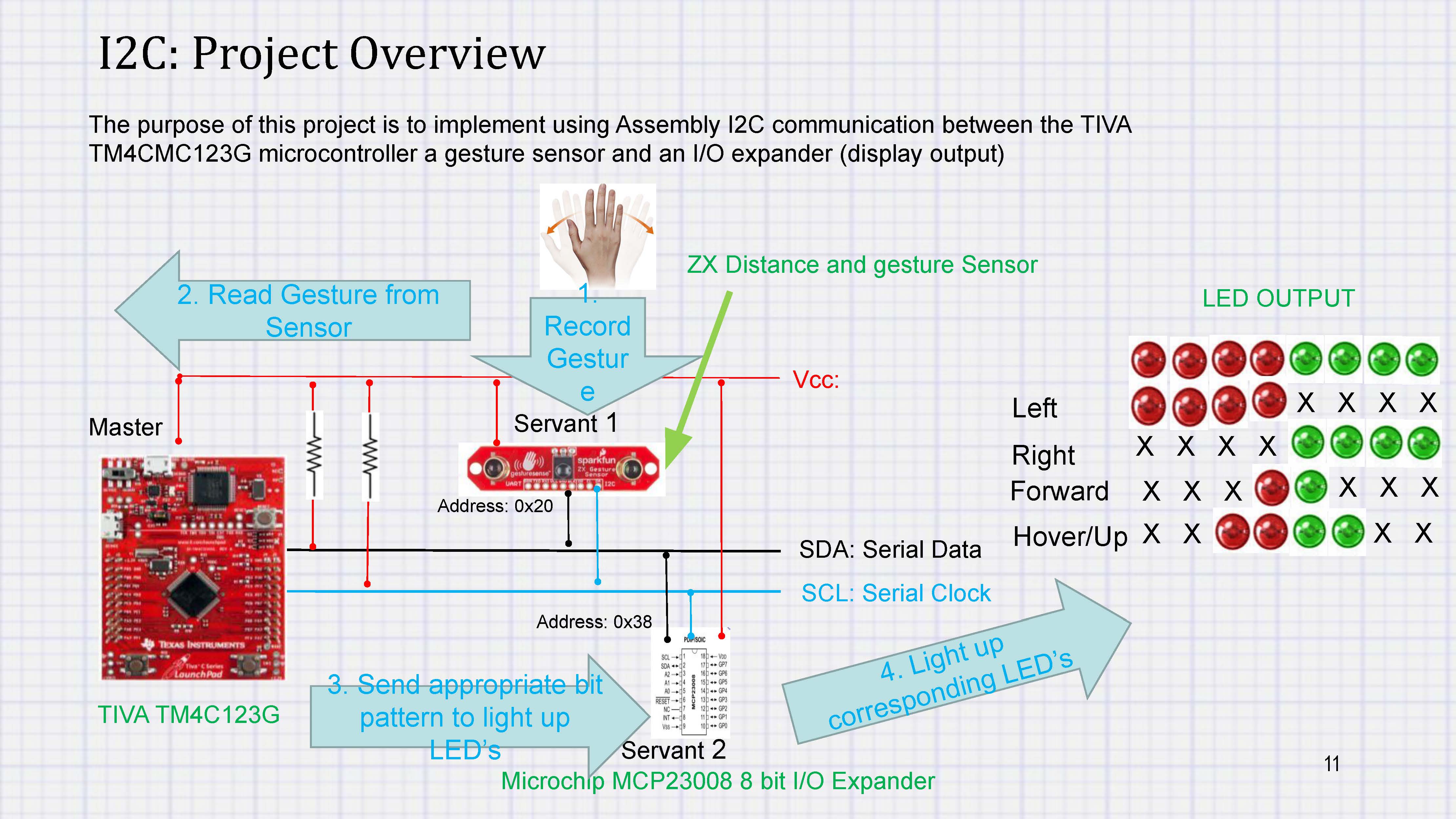
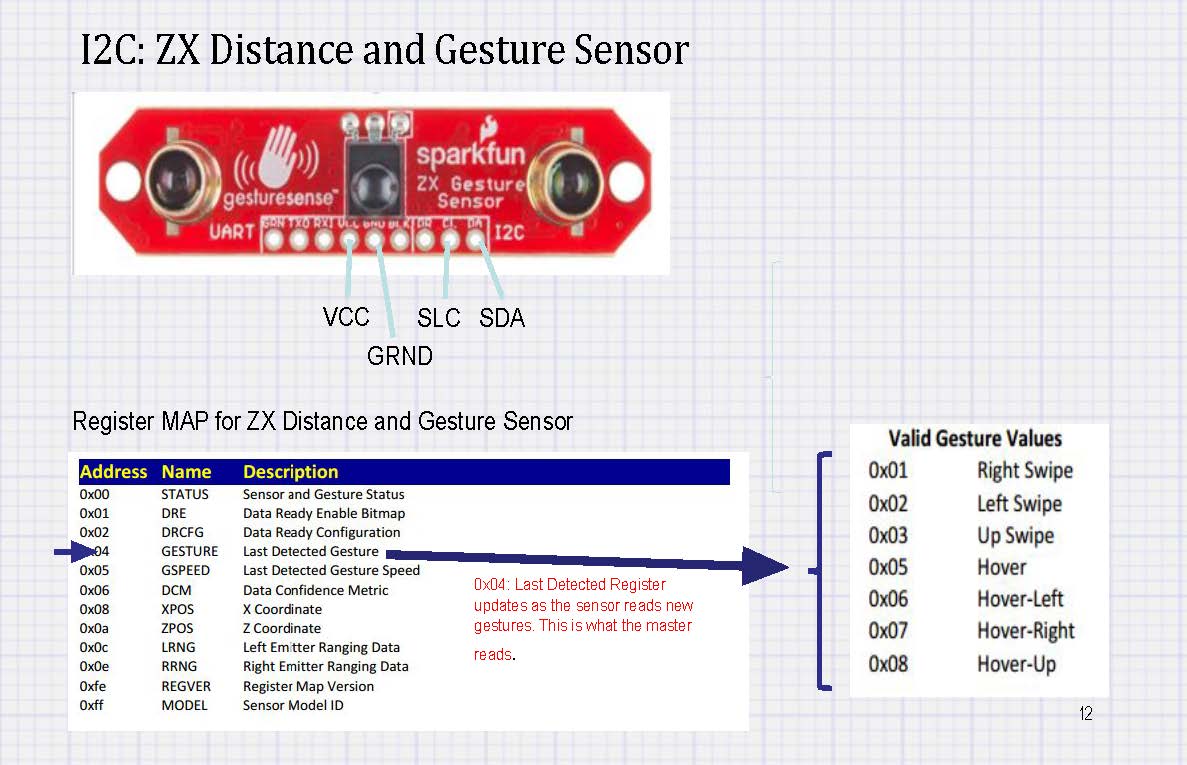
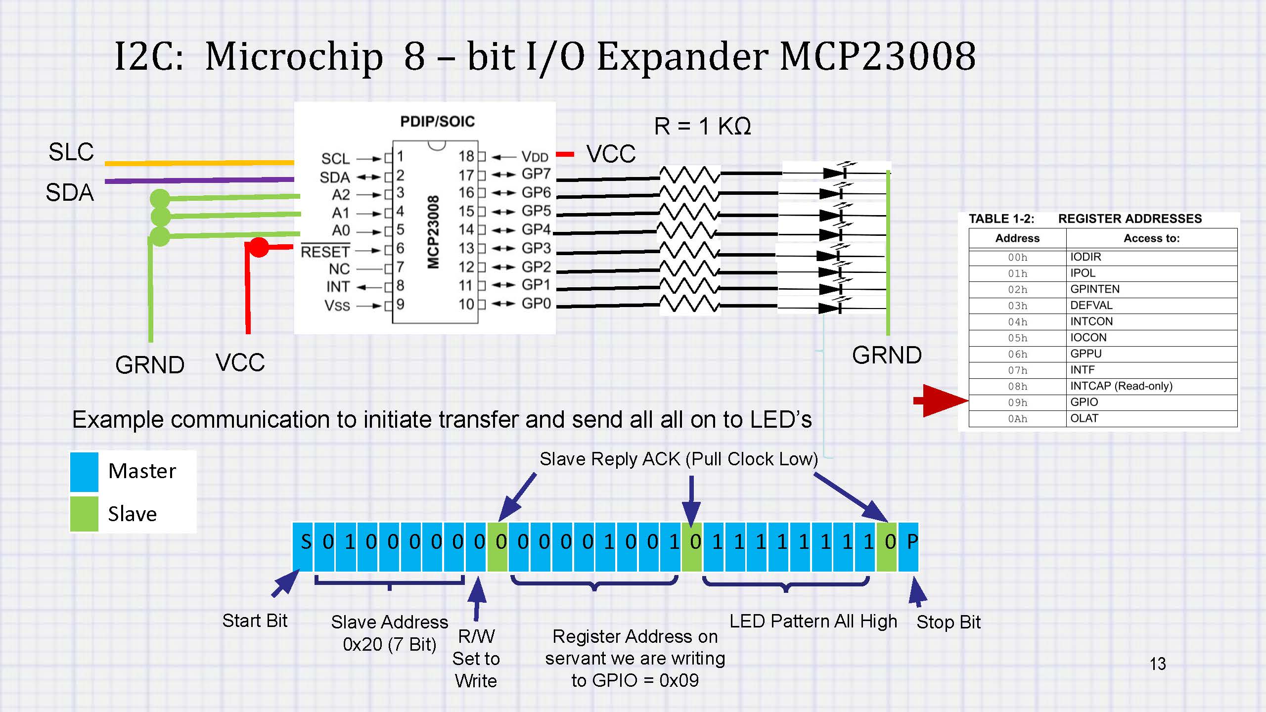
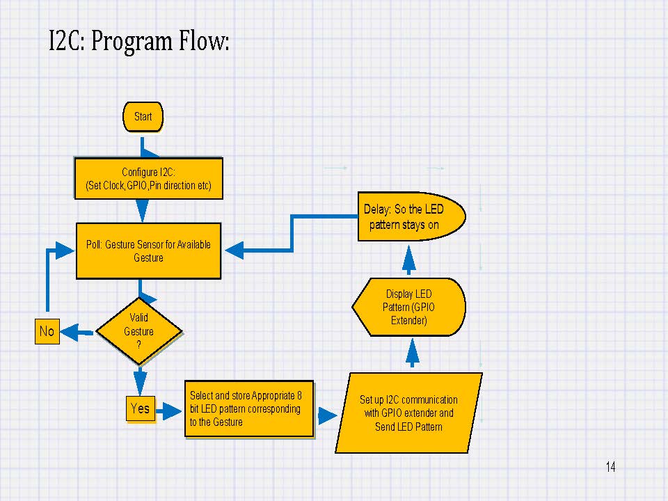
This project implemented I2C communication between a TI Tiva C Series (TM4C123G) board and a Sparkfun ZX Gesture Sensor. Gesture data was read from the sensor and stored in register 0x06 of the Tiva board. The values received and stored from the gesture sensor:
- 0x01: Right
- 0x02: Left
- 0x03: Up
- 0x04: Down

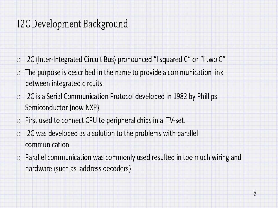
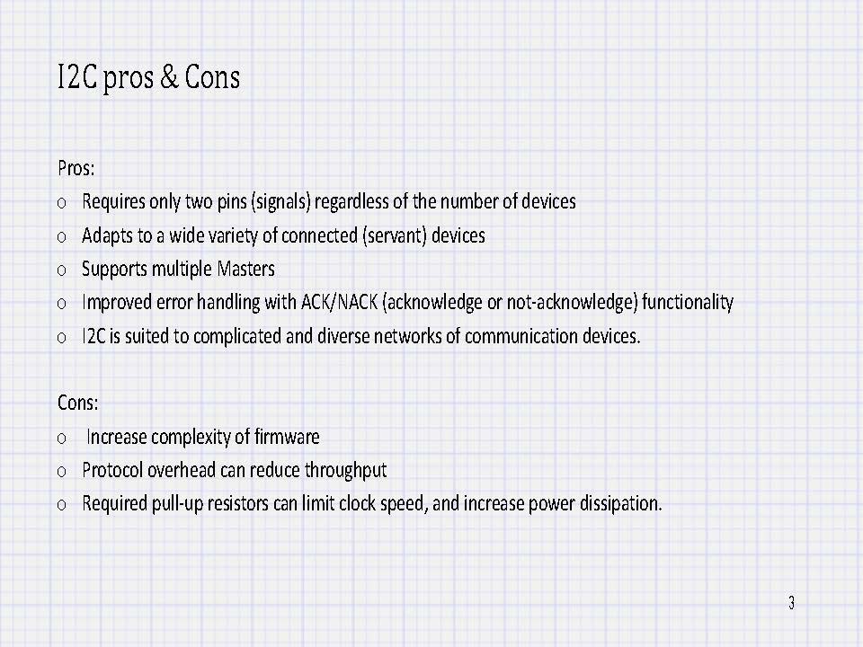
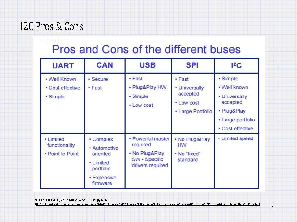
The slideshow below is the concluding presentation I delivered in class.
Description
Tom DesRosiers
This is the final individual project for the Advanced Microprocessors graduate course (EEE 5264) at Lawrence Technological University. The project demonstrates the implementation of a real world task using ARM assembly, which was the focus of the course.


Here is the final ARM assembly code I ran using the Kiel Embedded Development kit.
;/***************************************************************************
; * This code did work after setup to store a gesture result in Register 0x06
; * and then continue in a loop reading
; * the values. Performance was mixed as I stepped thru the code (in debug)
; * mode. 0x01 = Right Swipe; 0x02 = Left Switch; 0x03 = Up Swipe; 0x05 = Hover
; * The goal of this project was to link it with an i2c LED display.
; *****************************************************************************
AREA WORD, CODE, READONLY ;Code block WORD, code readonly
EXPORT __main ;Export function to other s file
ENTRY ;Entry point of main program
;System Control Registry map is on page 234 general map is on page 92
; page 1017 register map of I2C
RCGCI2C EQU 0x400FE620 ;Page 348
RCGCGPIO EQU 0x400FE608 ;Page 340
GPIOAFSEL EQU 0x40004420 ;Page 671
GPIODEN EQU 0x4000451C ;Page 682
GPIOODR EQU 0x4000450C ;Page 676
GPIOPCTL EQU 0x4000452C ;Page 688
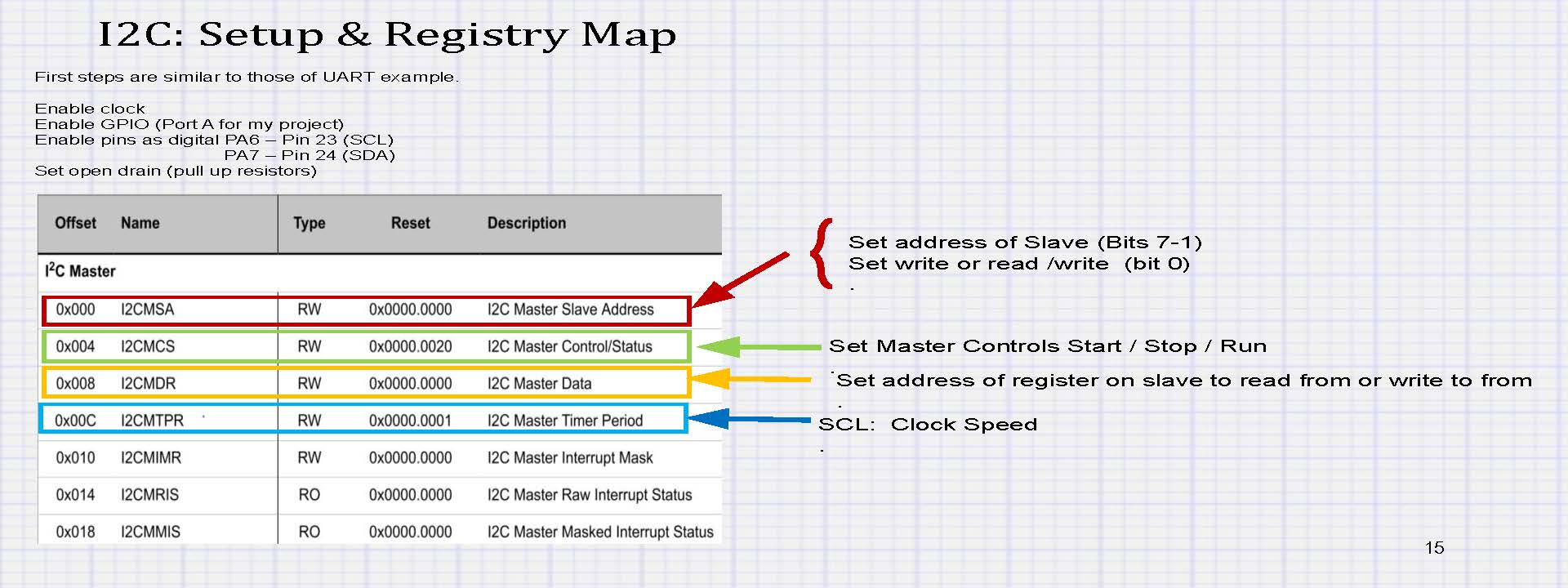
I2CMCR EQU 0x40021020 ;Page 1031
I2CMTPR EQU 0x4002100C ;Page 1026 - Remember i2c1
I2CMSA EQU 0x40021000 ;Page 1019 - Remember i2c1
I2CMDR EQU 0x40021008 ;Page 1025 - we are using i2c1
I2CMCS EQU 0x40021004 ;Page 1020 - we are using i2c1
__main
;***** SET UP I2C COMMUNICATION *******************
;*1 Enable the i2c clock using the RCGCI2C Inter-Integrated Circuit Run Mode
;Clock Gating Control register the System Control Module Page 348 Datasheet
LDR r0, =RCGCI2C ;Load the address of the RCGCI2C register in r0
LDR r1,[r0] ;Load the contents of the RCGCI2C register in r1
ORR r1,#0x2 ;Set bit "1" of RCGCI2C to enable I2C module 1
STR r1,[r0] ;Store r1 back into the register
;*2. Enable the clock to the appropriate GPIO module via the RCGCGPIO register
;in the System Control Module(page 340).See table 23-5 page 1351 and page 341
LDR r0, =RCGCGPIO ;Load the address of the RCGCGPIO register in r0
LDR r1,[r0] ;Load the contents of the RCGCGPIO register in r1
ORR r1,#0x1 ;Set bit "1" of RCGCGPIO to enable "GPIO Port A" Clock
STR r1,[r0] ;Store value back into RCGCGPIO
;3 Enable appropriate pins alternate function using the GPIOAFSEL
;register (pg671) Chart on page 1346 i2c module 1 uses pins 23 (SCL)
;and 24 (SDA) diagram page 1328Pin 23 = PA6 and pin 24 is PA7.
;GPIO ALternate Function Select
LDR r0, =GPIOAFSEL
LDR r1,[r0] ;Load the contents of the GPIOAFSEL register in r1
ORR r1,#0xC0 ;Set bit "6" and Bit "7" corresponding to PA6 and PA7.
STR r1,[r0] ;Store r1 back into the register
;*Enable pins for digital functionality pg 682 register
;GPIODEN-GPIO DIGITAL ENABLE
LDR r0, =GPIODEN
LDR r1,[r0] ;Load the contents of the GPIODEN register in r1
ORR r1,#0xC0 ;Set bit "6" and Bit "7" corresponding to PA6 and PA7.
STR r1,[r0] ;Store r1 back into the register
;*4.Enable I2CSDA(DATA) which is PA7 for open-drain operation
;pg 676-GPIO IOen Drain Select GPIOODR
LDR r0, =GPIOODR
LDR r1,[r0] ;Load the contents of the GPIODEN register in r1
ORR r1,#0x80 ;We need enable the data bit PA7.
STR r1,[r0] ;Store r1 back into the register
;*5 Configure PMCn fields in the GPIOPCTL reg to assign I2C signals to the
;appropriate pins page 688 Table 23-5 pg 1351 From page 1351 Look at the
;table for PA6 -pin23 ->3 and PA7 -pin24 ->3
LDR r0, =GPIOPCTL
LDR r1,[r0] ;Load the contents of the GPIOPCTL register in r1
ORR r1,#0x33000000 ;Load a three 3 in PA6 and a 3 in PA7
STR r1,[r0] ;Store r1 back into the register
;*6.Initialize I2C as a Master by writing the I2CMCR (i2c configuration)
;register with a value of 0x0000.0010. Pin 4 set We are using i2C 1 this
;is on page 1031. Pin 4 = "I2c Master Function Enable."Set this to 1
LDR r0, =I2CMCR
LDR r1,[r0] ;Load the contents of the I2CMCR register in r1
ORR r1,#0x10 ;Set bit 4 of this register
STR r1,[r0] ;Store r1 back into the register
;*7. Set the desired SCL clock speed of 100 Kps by writing the I2CMTPR register
;with the correct value. The value written to the I2CMTPR register
;represents the number of system clock periods in one SCL clock period.
; TPR = (SYSTEM CLOCK/(2*(SCL_LP + SCL_CLK)) -1
; TPR = (20 MHz / (2*(6+4)*100,000))-1;
; TPR = 9
; For our device the clock is 80 MHZ so the value is 0x27 from chart
;Write the I2CMTPR page 1026.
LDR r0, =I2CMTPR
LDR r1,[r0] ;Load contents of the I2CMTPR register in r1
AND r1,r1,#0xFFFFFF80 ;Save current values of registers from position
;7-1 and clear out the rest of the bits.
ORR r127 ;Set value of the timer period 0x27 for 80 MHz
STR [r1] ;Store r1 back into the register
;Initial set complete This establishes the I2C, you can perform communication
Loop5 ;main l
;Call Function ReadGestureSensor to fill the Read Gesture in r6
BL ReadGestureSensor
NOP ;Test
B Loop5 ;End of Main L
;END MAIN LOOP
;---------------------------------------------------------------------------
; Function: ReadGestureSensor
; This function should be called after i2c is set up
; This function Reads the 0x04 (address) on the gesture sensor
; and stores the value in register 0x6
;--------------------------------------------------------------------------
ReadGestureSen
;8.SET SLAVE ADDRESS: Specify the slave address and that the next operation
;is a receive by writing to I2CMSA Page 1019 - I2C Master SLave Address.
;Slave address of GESTURE SENSOR is 0x38 the slave address takes up bits
;7 down to 1 0x38 shifted to the right once is = 1C 1C = 0001.1100
;Bit zero dictates Receive/Send ="0 is transmit and 1 is receive.For this case
;we are transmitting so zero is set." We will set it below.Send the address
;of the slave device we are writing (a register address) to the slave device
LDR r0, =I2CMSA ;I2CMSA Mater Control/Status register pg 1019
LDR r1,[r0] ;Load the contents of the I2CMSA register in r1
AND r1,r1,#0xFFFFFF01 ;Values for the Slave address goes from bits 7-1.
ORR r1,#0x20 ;Set address=0x10 from bit 7-1 and 0 = Transmit
STR r1,[r0] ;Store updated value
;Bit 0 of I2CMSA SET MODE WHETHER READ (RECEIVE)=1/OR WRITE (TRANSMIT)
;0 Set Whether this is a Receive (High) or Transmit (Low)
LDR r0, =I2CMSA ;I2CMSA Mater Control/Status register. pg 1020
LDR r1,[r0] ;Load the contents of the I2CMCS register in r1
AND r1, r1,#0xFFFFFFFE ;Preserve all values expect for the LSB
ORR r1,#0x0 ;Set 1 receive Bit zero of this register = 0
;Transmit and if it is = 1 it is
;receive. We Set it to TRANSMIT
STR r1,[r0]
;specify register to be read
;Write the Slave register to be read to I2CMDR register
LDR r0, =I2CMDR ;I2CMDR Mater Control/Status register
LDR r1,[r0] ;Load the contents of the I2CMDR register in r1
AND r1,r1,#0xFFFFFF00 ;Mask
ORR r1,#0x04 ;The register to be read from the sensor is "0x04"
STR r1,[r0]
;send control byte and register address byte to slave device
;Set Stop,Start,Run-0x3 to send the initial communication with slave device
;Set the initial conditions of the transfer the=Start and Run Bits
;need to be set in the I2CMCS registerThe last Five bits are
;4=HS (high Speed),3 = ACK (Acknowledge), 2 = Stop, 1 = Start, 0 = Run
LDR r0, =I2CMCS ;I2CMCS Mater Control/Status register
LDR r1,[r0] ;Load the contents of the I2CMCS register in r1
AND r1,r1,#0xFFFFFFF8 ;Mask
ORR r1,#0x3 ;SEND_START=Set bit 0 (Run) bit 1 (Start) bit 2 (Stop)
STR r1,[r0]
;11.***VERIFY TRANSACTION** Wait until ALL OF THE DATA IS SENT:
;the transmission completes by polling the I2CMCS registers BUSBSY(bit 6)
;until it has been CLEARED Value=0 the I2C is idle,Value=1 I2C bus is busy
LDR r0, =I2CMCS ;I2CMCS Mater Control/Status register
LDR r1,[r0] ;Load the contents of the I2CMCS register in r1
AND r1,#0x01 ;Clear out bits except for bit [0] by Masking with 0's
Loop CBZ r1, Exit
LDR r0, =I2CMCS ;I2CMCS Mater Control/Status register
LDR r1,[r0] ;Load the contents of the I2CMCS register in r1
AND r1,#0x01
B Loop
E
;12:Check ERROR bit 1 I2CMCS register the transmit acknowledged.
LDR r0,=I2CMCS
LDR r1, [r0]
AND r1,#0x02 ; Mask off unwanted bits (we want to keep bit 1)
Loop1 CBZ r1,Ex
;12:Check ERROR bit 1 I2CMCS register confirm transmit acknowledged.
LDR r0,=I2CMCS
LDR r1, [r0]
AND r1,#0x02 ; Mask off unwanted bits we want to keep bit 1
B Loop1
Exit1
;Specify that we are going to read from slave device
;Send address of the slave device specify that we are writing to the
;slave device
LDR r0, =I2CMSA ;I2CMSA Mater Control/Status register pg 1019
LDR r1,[r0] ;Load the contents of the I2CMSA register in r1
AND r1,r1,#0xFFFFFF01 ;Values for the Slave address goes from bits 7-1.
ORR r1,#0x20 ;Set address=0x10 from bit 7-1 bit 0 = Transmit
STR r1,[r0] ;Store updated value
;Bit 1 of I2CMSA SET WHETHER READ (RECEIVE)=1/OR WRITE (TRANSMIT) 0 Set Whether
;this is a Receive (High) or Transmit (Low)
LDR r0, =I2CMSA ;I2CMSA Mater Control/Status register. pg 1020
LDR r1,[r0] ;Load the contents of the I2CMCS register in r1
AND r1, r1,#0xFFFFFFFE ;Preserve all values expect for the LSB
ORR r1,#0x1 ;Set bit to 1 to establish receive Bit zero of this
;and if it is = 1 it is receive. We Set it to TRANSMIT
STR r1,[r0]
;Send control byte and read from the register we specified
;Set Stop,Start,Run-0x3 send initial communication with the slave device
;Set initial conditions of transfer case Start and Run Bits need to be set
;in the I2CMCS register the last Five bits are
;4 = HS (high Speed), 3 = ACK (Acknowledge), 2 = Stop, 1 = Start, 0 = Run
LDR r0, =I2CMCS ;I2CMCS Mater Control/Status register
LDR r1,[r0] ;Load the contents of the I2CMCS register in r1
AND r1,r1,#0xFFFFFFF8 ;Mask
ORR r1,#0x7 ;CMD_SINGLE_RECEIVE=Set bit 0(Run) and bit 1(Start)
;and bit 2 (Stop)
STR r1,[r0]
;*** VERIFY TRANSACTION **Wait for MCU to finish transaction
;11.Wait until ALL OF THE DATA IS SENT:transmission completes polling
;the I2CMCS registers BUSBSY (bit 6) until it has been CLEARED
;Value = 0 the I2C is idle, Value = 1 The I2C bus is busy
LDR r0, =I2CMCS ;I2CMCS Mater Control/Status register
LDR r1,[r0] ;Load the contents of the I2CMCS register in r1
AND r1,#0x01 ;Clear out all bits except for bit [0] by Masking with 0's
Loop2 CBZ r1, Exit2
LDR r0, =I2CMCS ;I2CMCS Mater Control/Status register
LDR r1,[r0] ;Load the contents of the I2CMCS register in r1
AND r1,#0x01
B Loop2
Exit2
;12:Check ERROR bit 1 in I2CMCS register confirm the transmit was acknowledged.
LDR r0,=I2CMCS
LDR r1, [r0]
AND r1,#0x02 ;Mask off unwanted bits (we want to keep bit 1)
Loop3 CBZ r1,Exit
;12:Check ERROR bit 1 in I2CMCS register to confirm transmit was acknowledged.
LDR r0,=I2CMCS
LDR r1, [r0]
AND r1,#0x02 ;Mask off unwanted bits we want to keep bit 1
B Loop3
Exit
;Return data pulled from the specified register
LDR r0, =I2CMDR ;I2CMDR Mater Control/Status register
LDR r6,[r0] ;Load the contents of the I2CMDR register in r1
BX LR
;************END OF FUNCTION ReadGestureSensor*************
END ; End of File GestureCodeSensor